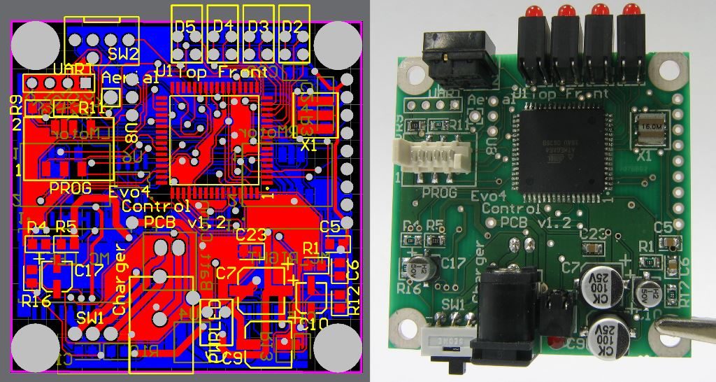
Are you thinking about designing a printed circuit board? PCBs are quite complicated, and you need to make sure that the layout that you choose is going to operate as well as you want it to. For this reason, we have put together some top tips for PCB design layout. Keep reading if you would like to find out more about this.

Leave Enough Space
One of the most important design tips for PCB layout is that you need to make sure that you are leaving enough space between the components. While many people might think that packing components closely is the best route to take, this can cause problems further down the line. This is why we suggest leaving extra space for the wires that will spread. This way, you’ll have the perfect PCB design layout.
Print Out Your Layout
Struggling to find out if your components sizes match? Our next tip is to print out your layout and compare the printed version to your actual components. Datasheets can sometimes come with errors, so it doesn’t hurt to double check the sizes in real life. If you take some time to do this, you can be sure that the sizes will match.
Think About Width Of Line
When you are deciding the width of the lines in your PCB design, you should make sure that you are choosing this based on the current. If you have a larger current flowing through the lines, then you should make sure to adapt your design to suit this. There are some online calculators that you can use to help make this decision.
Talk To Your Manufacturer
If you spend a long time working on your PCB design project before you have spoken to a manufacturer then you might find that you come across some problems. You need to find out about any specifications that they might have that could affect the design of your project. Use their guidelines to create your design and you’ll find things a lot simpler further down the line.
Compare Your Schematic
Our final tip for those who want to improve their PCB design layout is to compare the layout to the original schematic. You have spent time working on your schematic for a reason so make sure to utilise the tools that allow you to directly compare these. This way, you can be sure that your layout matches what you need for this particular project.
Final Verdict
If you are going to be working on PCB design project in the near future, make sure to take on board all of the tips that we have given you in this article. Think about leaving enough space between your components and considering the width of your lines. You should also make sure to talk with your manufacturer about their specifications before going ahead with the project. This way you’ll have a successful design that will help to create a working PCB.
The post Top Tips For PCB Design Layout appeared first on The Crazy Programmer.
No comments:
Post a Comment